
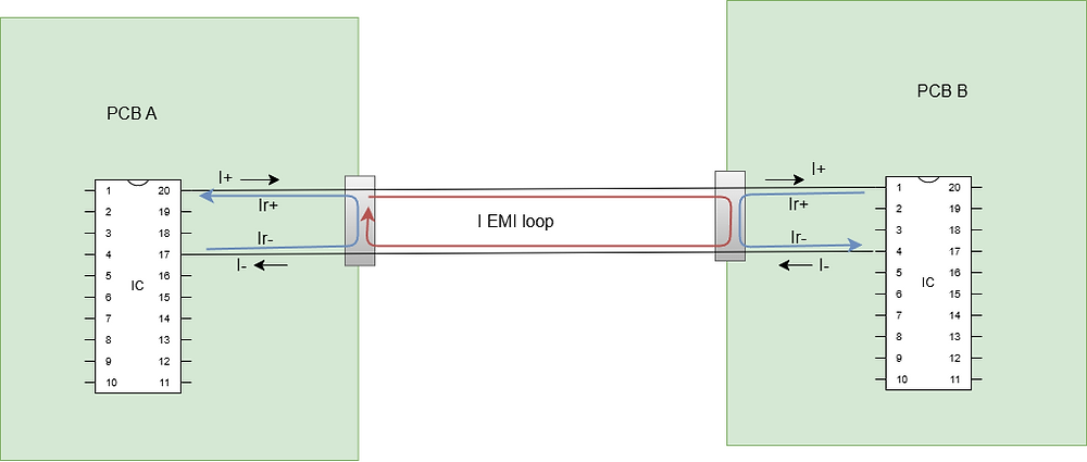
The RS422 and RS485 standards are well known in the industry for their reliability and noise immunity.
However, they do hide the seeds for narrowband emissions, at least in some industries like for example the defense industry when you need to meet the MIL STD 461, and the tollerated radiated emission is lower compared to other standards.
RS22 may create an unique problem.
The purpose of this blog is to discuss an error that may occur if you are not careful when designing the return current path on your RS422 (RS485) driver if you are not careful during the design phase.
Let'e consider the case where we have 2 PCBs connected with cable as shwon in the drawing below.
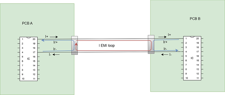
For the sake of this example, let's assume that we have a perfect PCB layout, where each track has a GND plane underneath it. The majority, if not all, of the return current, from the I+ in this case, will flow to the track below the I+. In this case, I have referred to this current as Ir+.
On the I- current, the same thing happens as well. A return current will be found below that track, and it will be referred to as Ir-.
Are we going to see anything interesting at the connection join?
The Ir+ current will somehow "join" the Ir- current pretty much in the same way that the Ir- current has joined the Ir+ current.
Both connectors will be affected by this.
There will be a current loop as a result of this (which I have referred to as an EMI loop) which may cause EMI interference in some cases.
Firstly, it is important to keep in mind that the wider the EMI loop, the greater the amount of EMI emission that will be emitted from it. Therefore, we need to introduce some design techniques that will minimize the negative effects of this.
The first thing you need to keep in mind is that the current loop that occurs at the PCB level (which is the loop made by Ir+ and Ir-) causes narrowband emissions to occur.
What is the best way to eliminate the problem?
The simplest way to route the differential trace is to route it at the closest point possible to the differential trace. This may be a topic that you have read about in a lot of books, but I hope that after reading this article you will also understand why and how it can affect narrowband EMI emissions.
The second emissions is created by the cable. However this is also very easy to fix
Twist the cables!
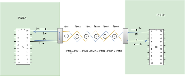
EMI loops on twisted cables are the sum of many loops.
The idea behind twisted cable is to have a lot of smaller magnetic loops so that the result is a smaller magnetic loop sum. The only known disadvantage of twisted cable is that it is more expensive.
I hope you enjoyed, and I hope after reading this article I managed to remove away some of the "black magic" behind twisted cables and reason behind place differential track as close as possible at PCB level.
Written by Francesco Poderico
More on EMC
EMC
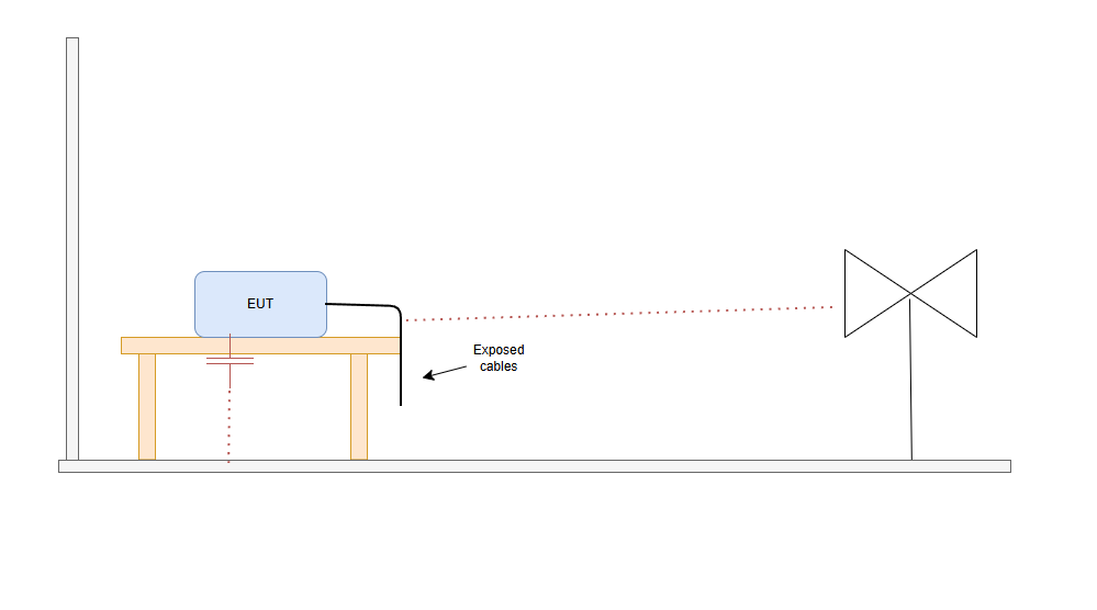
Why Moving the EUT Changes the Emissions Plot
1. Introduction – why a small change can make great differences in the plot Did this happen to you. You go to the testing lab. you do a full RE scan and the scan looks great. Then you - Rotate the EUT 90° - Lift a cable - Move the EUT by 20 cm - Change cable routing And the emissions plot change
Francesco Poderico · · 3 min read
EMC
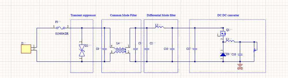
Power Supply Emissions: How I Separate Differential Mode from Common Mode
When I debug EMC problems on a DC/DC converter, I use a very simple test to understand whether the dominant mechanism is Differential Mode (DM) or Common Mode (CM). The test is simple: I increase the load and observe what happens to the emissions. If: - The peak frequencies stay the same,
Francesco Poderico · · 3 min read
EMC
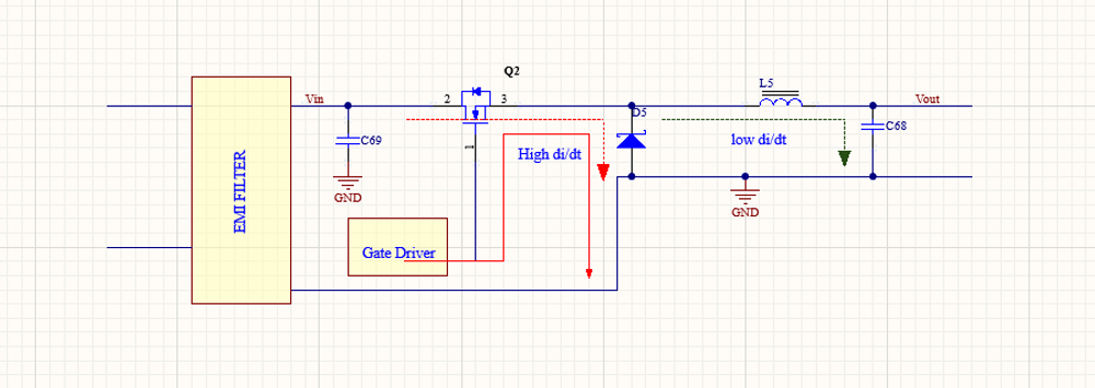
Identifying Low di/dt and High di/dt Currents in DC‑DC Converters
Introduction In switch‑mode DC‑DC converters, not all currents are equal from an EMC, signal integrity, or reliability perspective. A critical distinction must be made between low di/dt current paths and high di/dt current paths. Misidentifying these paths is one of the most common root c
Francesco Poderico · · 4 min read