
Introduction
In switch‑mode DC‑DC converters, not all currents are equal from an EMC, signal integrity, or reliability perspective. A critical distinction must be made between low di/dt current paths and high di/dt current paths. Misidentifying these paths is one of the most common root causes of excessive EMI, poor efficiency, unstable switching behaviour, and failed compliance tests.
This article focuses on:
-
How to correctly identify high di/dt and low di/dt current loops in DC‑DC converters
-
Why high di/dt currents dominate EMI behaviour
-
Practical mitigation techniques
-
The often underestimated role of gate driver selection and layout
The discussion applies to buck, boost, and isolated topologies.
What di/dt Really Means in a DC‑DC Converter
di/dt is the rate of change of current with time. In switching power supplies, fast transitions are unavoidable, but where those transitions flow is what matters.
-
High di/dt paths: Currents that change rapidly during switching transitions (typically nanoseconds)
-
Low di/dt paths: Currents that change slowly or are continuous (typically dominated by inductance)
From an EMC standpoint, voltage noise is often a consequence of uncontrolled current transitions interacting with parasitic inductance:
V = L * di/dt
Even a few nH of parasitic inductance becomes problematic when di/dt is high.
Identifying High di/dt Current Loops
High di/dt loops are almost always associated with the switching action itself. These loops are typically small in ideal schematics but large in real PCB layouts.
Typical High di/dt Loops (Buck Converter Example)
-
Input switching loop
-
High‑side MOSFET
-
Low‑side MOSFET (or diode)
-
Input capacitor (Cin)
-
-
Gate drive loop
-
Gate driver output
-
MOSFET gate
-
MOSFET source return
-
-
Switch node capacitances
-
MOSFET Coss
-
Parasitic capacitance to ground or heatsink
-
These loops conduct sharp current pulses during every switching transition.
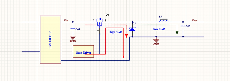
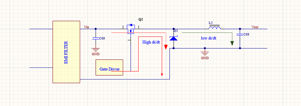
example of high di/dt and low di/dt current pats.
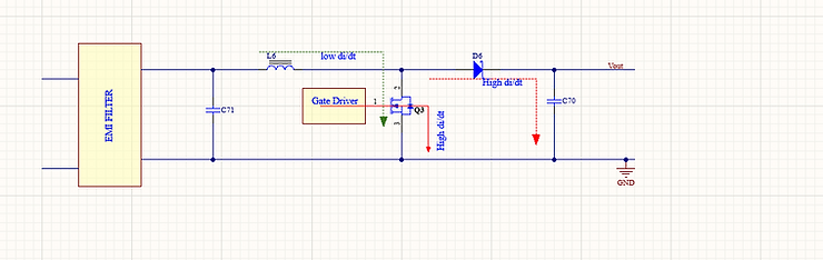
another example of low and high di/dt paty. notice the gate driver may requires ampers. so it creates a high di/dt path
Key Identification Rule
If a current path conducts only during switching edges, assume it is high di/dt and treat it as EMI‑critical.
Identifying Low di/dt Current Paths
Low di/dt currents are generally shaped by inductance and load demand rather than switching speed.
Typical low di/dt paths include:
-
Output inductor current
-
Load current paths
-
Bulk input current (after local decoupling)
These paths are important for efficiency and thermal design, but they are not the primary EMI aggressors.
A common mistake is over‑optimising these paths while neglecting the true high di/dt loops.
please notice we are interested in high di/dt not high current
Why High di/dt Paths Dominate EMI
High di/dt currents:
-
Generate broadband noise
-
Excite PCB parasitic inductances
-
Couple capacitively and inductively into other circuits
-
Create common‑mode noise through parasitic capacitances
This explains why EMI issues often persist even when switching frequency is relatively low.
EMI is driven more by edge speed than frequency.
Mitigation Strategies for High di/dt Currents
1. Minimise Loop Area
The single most effective mitigation technique.
-
Place input capacitors as close as physically possible to the MOSFETs
-
Use wide, short copper planes instead of thin traces
-
Avoid vias in high di/dt loops where possible
Rule of thumb: If you can draw the loop with a pen, it is probably too large.

Once you have identified the high di/dt loop. minimize the loop. 2. Control di/dt, Not Just Frequency
Reducing edge speed reduces EMI at the source.
Methods include:
-
Gate resistors (carefully selected)
-
Slew‑rate‑controlled gate drivers
-
Adaptive dead‑time control
Have you ever seen a one ohm resistor on a gate? or a ferrite on a gate ?
The designer was trying to reduce the di/dt an that loop!
However, slowing edges too much increases switching losses. This is a controlled trade‑off, not a blanket fix.
REMEMBER THE HEAT ! ... adding serie resistor on gates will increase the overall temperature
3. Proper Gate Driver Selection – A Critical Factor
Gate drivers directly control how fast current transitions occur in the power stage.
Key gate driver parameters that matter:
-
Peak source and sink current
-
Output impedance
-
Propagation delay matching
-
Ability to drive large Qg MOSFETs cleanly
An under‑specified gate driver often causes:
-
Excessive di/dt due to uncontrolled ringing
-
Gate bounce and false turn‑on
-
Increased common‑mode noise
Conversely, an over‑aggressive driver can worsen EMI if not paired with correct layout and damping.
4. Gate Loop Layout Is as Important as the Driver
Even the best gate driver will fail if the gate loop is poorly designed.
Best practices:
- Extremely short gate‑source loop
The gate loop is itself a high di/dt loop and must be treated accordingly.
5. Damping and Snubbing
Where layout and gate control are insufficient:
-
RC snubbers on the switch node (see other articles on the subjects)
-
Ferrite beads on gate (with caution)
-
Split gate resistors (turn‑on vs turn‑off control)
These should be used as fine‑tuning tools, not primary fixes for poor current loop design.
Practical Identification Workflow
A reliable approach when reviewing a design:
-
Highlight all switching devices
-
Identify which currents flow only during transitions
-
Draw the smallest possible loop those currents should take
-
Compare with the actual PCB layout
-
Prioritise fixing mismatches
This process is far more effective than blind EMI filtering later.
Conclusion
Correctly identifying high di/dt versus low di/dt current paths is foundational to good DC‑DC converter design. High di/dt currents dominate EMI behaviour, stress components, and expose layout weaknesses.
Mitigation starts with:
-
Accurate current loop identification
-
Aggressive loop minimisation
-
Thoughtful gate driver selection
-
Gate loop layout treated as a first‑class design concern
Written by Francesco Poderico
More on EMC
EMC
Why Moving the EUT Changes the Emissions Plot
1. Introduction – why a small change can make great differences in the plot Did this happen to you. You go to the testing lab. you do a full RE scan and the scan looks great. Then you - Rotate the EUT 90° - Lift a cable - Move the EUT by 20 cm - Change cable routing And the emissions plot change
Francesco Poderico · · 3 min read
EMC
Power Supply Emissions: How I Separate Differential Mode from Common Mode
When I debug EMC problems on a DC/DC converter, I use a very simple test to understand whether the dominant mechanism is Differential Mode (DM) or Common Mode (CM). The test is simple: I increase the load and observe what happens to the emissions. If: - The peak frequencies stay the same,
Francesco Poderico · · 3 min read
EMC
Why Placing a Ground Plane Under a Common-Mode Choke Often Makes EMI Worse
This is one of the most common layout mistakes I see during EMC reviews. The schematic is correct.The common-mode choke is correctly placed at the interface. But the PCB layout shows a solid ground plane directly underneath the choke. Imagine a GND plane below the chocke. The intention is usua
Francesco Poderico · · 3 min read