
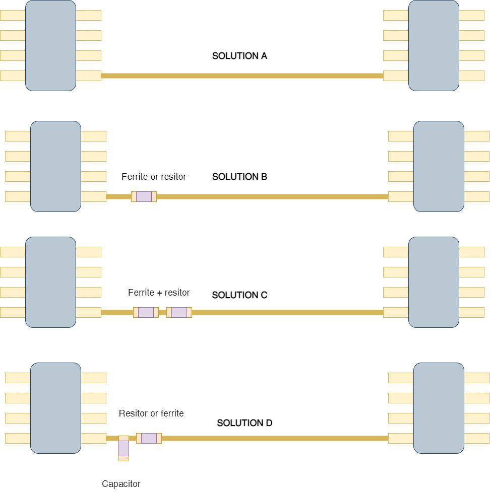
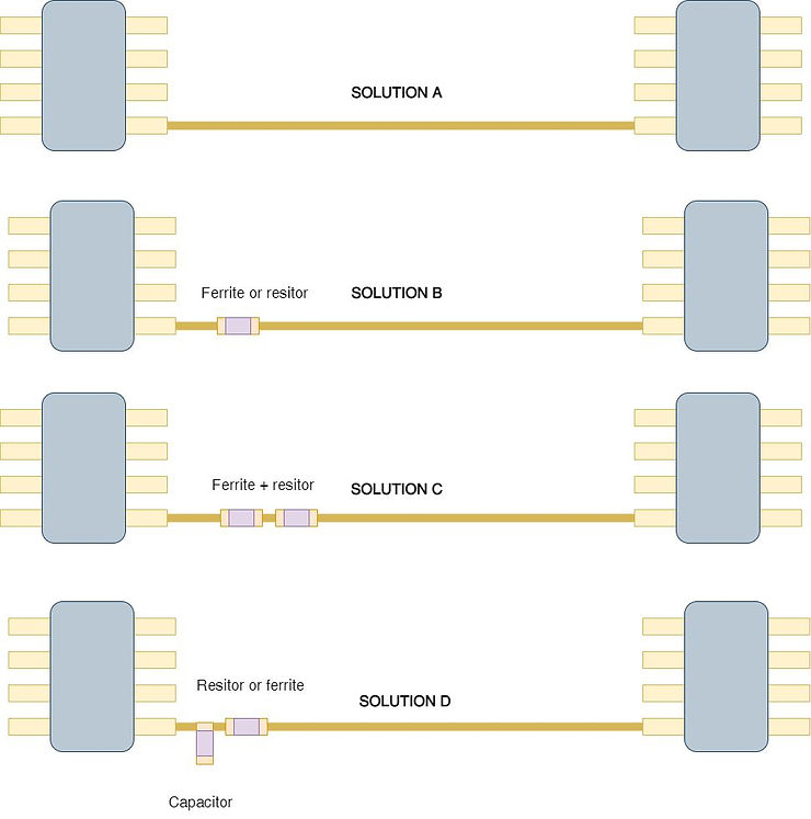
Some time ago, I wrote a blog post about the design technique I use when I am solving EMC emissions for clients when I am working on their projects. As a result of some comments (from LinkedIn), I feel that the subject is not fully understood by the majority of people. As a result, I decided to rewrite the original post to clarify a few points so that it would be easier to understand.On occasion, when we route clocks on a PCB from A to B, we encounter one of the following problems as a result:1. partial reflection2. ringing3. none of the two above but emissions above the limitsThroughout the entire design process, I make sure that flexible solutions are applied consistently. For example, I place filters in strategic places of the device (I may not fit all of them unless I believe that I actually need them), which allows me to fix issues with minimal changes and reduce the time of the compliance testing for EMC.If I am routing a clock, for example, I implement solution D in almost all of my designs, even if the trace is very short.As shown in solution D, I begin with a not-fitted capacitor and a 0-ohm resistor, and proceed from there.In my career, I have never implemented Solution A (although I have seen my customers do this); however, I have seen Solutions B and C many times in books and articles that I have read. In spite of this, I only implement Solution D because it is the most flexible and it has always worked for me.I would like to begin with the even harmonics of the waveform.For instance, let us imagine that we are performing an EMC test, that our clock is 25 MHz, and that we are seeing harmonics at 100 MHz, 200 MHz, etc. Is there anything that can cause even harmonics to occur? The reflections! Consequently, due to reflection, the clock will have a larger number of even harmonics, and as a result, the return wave, when "hit" on the clock side, may generate an RF emission that will result in the emission of 100 MHz and 200 MHz.This is the reason why I fit a resistor of 0 ohms near the clock so that a link resistor can be connected! If I see some even harmonics during the EMC test, I change the resistor from 0 to 10-30 ohm, and so far, I have solved the problem in 100% of the cases where I have encountered it.Is it possible to get odd harmonics as well?I think you have either selected a clock that has a higher fanout than you need, or the trace should have a larger capacitive load than it does.You should try to shape the rising and falling edge of your clock without increasing the rise and fall time of your clock. It is usually enough to control the emissions with a capacitor, as shown in Solution D. Usually, 10-20 pF is enough to control the emissions.In my previous post (from LinkedIn), some people assumed that the capacitor was after the resistor, this is incorrect. The solution is very anti-intuitive; the capacitor is there since our trace is not capacitive enough and the "clock" has an edge too sharp.What about if we have ringing and an overshoot? This may add emission at the resonance frequency of the oscillations.Some people use a dumper resistor, but I don't like it, I prefer using just a ferrite that has a higher resistive value at the oscillation frequency.For example, if we are using a 25MHz clock and the overshooting is at 111.2 MHz, a ferrite with a resistor value of at least 50 ohms @ 100MHz should be enough. please notice I said resistor value, not impedance!
Post Button
Chat
loadbalancer.visitor-analytics.io
loadbalancer.visitor-analytics.io is blocked
Written by Francesco Poderico
More on PCB
PCB
EMC Troubleshooting Part 3 — Broadband Footprints: 2‑Layer Boards & Plane Slots
Scope: Why some products show broadband radiated emissions from 30 MHz–1 GHz, why issues often persist up to 400 MHz–1 GHz even on multilayer boards, and how to prove and fix the root cause fast. 1) What “broadband” really means in RE On the plot, broadband looks like a wide hum
Francesco Poderico · · 4 min read
PCB
High-Speed Vias: Why Solid Ties Beat Thermal Reliefs
Thermal-relief “spokes” help solderability, but they add inductance and cut slots in your reference plane—exactly where high-frequency return current needs a short, wide path. For HDMI, PCIe, and other multi-GHz links, prefer solid connections to ground on anything that carr
Francesco Poderico · · 2 min read

PCB
Conductive Immunity failure due to a two layers stack PCB
Over the last ten years, I have seen so many PCBs fail conductive immunity that I could write a book about it. In most cases, the errors are caused by bad designs and a lack of understanding of the ground plane's role. Since I keep seeing people recommend designing 2 layers PCBs to save a few pence,
Francesco Poderico · · 2 min read