
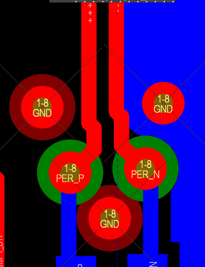
Thermal-relief “spokes” help solderability, but they add inductance and cut slots in your reference plane—exactly where high-frequency return current needs a short, wide path. For HDMI, PCIe, and other multi-GHz links, prefer solid connections to ground on anything that carries RF return (stitching vias, connector grounds, shields, EP/PowerPAD vias). Keep thermals only where assembly truly demands them.
Why I avoid thermals on RF returns
I don’t skip thermals because I’m lazy; I skip them because I’ve seen the surprises they cause below 1 GHz and well into the GHz range. A thermal relief connects a pad to a plane with a few narrow spokes. Those spokes add series inductance, and the clearance ring carves a slot in the plane. Measured/modelled work puts a typical thermal’s inductance in the tens to a few hundred picohenries; tiny in DC terms, but at GHz it becomes ohms of reactance. Example: 200 pH at 3 GHz ≈ 3.77 Ω; 0.1 nH at 6 GHz ≈ 3.77 Ω; 1 nH at 1/3/6 GHz ≈ 6.28/18.85/37.70 Ω—enough to force return current to detour and radiate.
- High-frequency impedance is dominated by XL=2πfL , not DC resistance. Shrink L , and the return current hugs the plane right under your trace.
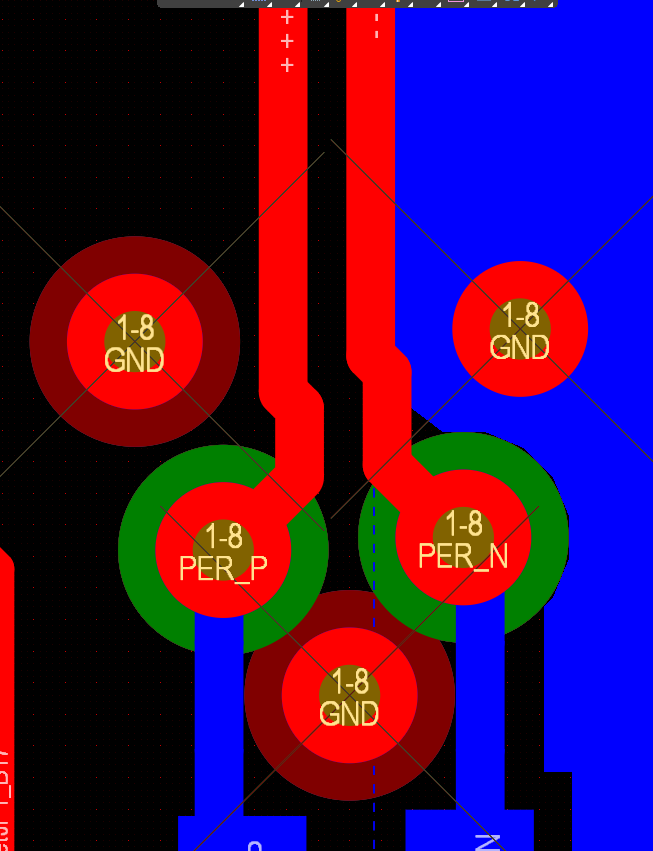
Details of vias on PCI-E PER lines
The slot-resonance trap (it’s not just vias)
Thermals don’t only choke vias; they also create short slots that can excite slot-wave resonances in launch/connector pads (think SMA/HDMI shells), producing the classic “mystery notch” in IL/RL. Best practice: avoid thermals in launch/return pads, or make the slot so short its resonance sits well above your signal bandwidth.
Why this really matters at HDMI/PCIe speeds
-
HDMI 2.0 : up to 6 Gb/s per channel (18 Gb/s aggregate).
-
HDMI 2.1 : up to 12 Gb/s per lane (48 Gb/s aggregate).
-
PCIe: Gen-4 16 GT/s, Gen-5 32 GT/s, Gen-6 64 GT/s (PAM4). Those lane rates push strong energy into the low/mid-GHz region where thermal-relief inductance hurts most.
When to use solid ties (no thermals)
Use solid connections anywhere the copper’s job is RF return, not “thermal isolation”:
-
Stitching vias at layer changes. Place two GND stitch vias flanking each differential-pair via pair (≈0.3–1.0 mm away) so the reference hand-off is tight and low-inductance.
-
Connector grounds & shells. Keep HDMI receptacle grounds, SMA grounds, and shield pads solid-tied to planes to prevent slot modes.
-
EP/PowerPAD via arrays. Vendors explicitly recommend solid ties to ground planes (no thermal webs) for thermal and EMC performance.
-
Via fences / ground frames. Close-spaced, solid-tied fences help contain fringing fields and provide many parallel return paths.
DFM note: Most power/ground vias do not need thermals—there’s no pin to solder in them. Use thermals only where a soldered component lead/pad would otherwise be starved of heat.
References & further reading
-
Thermal-relief impedance (DC→800 MHz): Boesman et al., Modeling the Low- and High-Frequency Impedance of Thermal Reliefs. (KULeuven Lirias; IMEC listing). Linias
-
Slot-mode resonances & thermals in launch pads: Eric Bogatin, Signal Integrity Journal. signalintegrityjournal.com
-
Stitching-via guidance & return hand-off: Altium docs/resources. Altiu m
-
DFM: vias usually don’t need thermals: Cadence PCB blog. resources.pcb.cadence.com
Written by Francesco Poderico
More on PCB
PCB
EMC Troubleshooting Part 3 — Broadband Footprints: 2‑Layer Boards & Plane Slots
Scope: Why some products show broadband radiated emissions from 30 MHz–1 GHz, why issues often persist up to 400 MHz–1 GHz even on multilayer boards, and how to prove and fix the root cause fast. 1) What “broadband” really means in RE On the plot, broadband looks like a wide hum
Francesco Poderico · · 4 min read

PCB
Conductive Immunity failure due to a two layers stack PCB
Over the last ten years, I have seen so many PCBs fail conductive immunity that I could write a book about it. In most cases, the errors are caused by bad designs and a lack of understanding of the ground plane's role. Since I keep seeing people recommend designing 2 layers PCBs to save a few pence,
Francesco Poderico · · 2 min read
PCB
Radiated emissions due to split planes.
As part of my job, I have been analyzing PCB layouts that have been designed by third parties. Whenever I do this, it is interesting to see what typical mistakes people make when they are doing this. As an example, for some reason, when there is a differential signal, such as USB, RS485, etc., peopl
Francesco Poderico · · 3 min read