
How Parasitic Capacitance Breaks Optocoupler Isolation in Switching Power Supplies
Francesco Poderico · · 3 min read
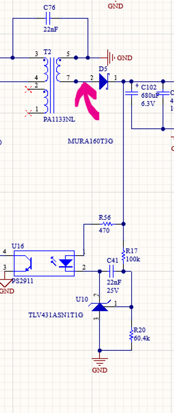
Optocouplers are widely used in isolated power supplies to transfer feedback information across an isolation barrier. In schematics, they appear as a clean and robust solution: no galvanic connection, clear separation between primary and secondary, and good noise immunity.
In practice, optocouplers are often one of the main entry points for switching noise into the control loop. They are commoinly used in isulated AC/DC, DC/DC and PoE applications.
This article explains why that happens, how parasitic capacitance plays a central role, and why small PCB layout details can completely undermine optocoupler performance.
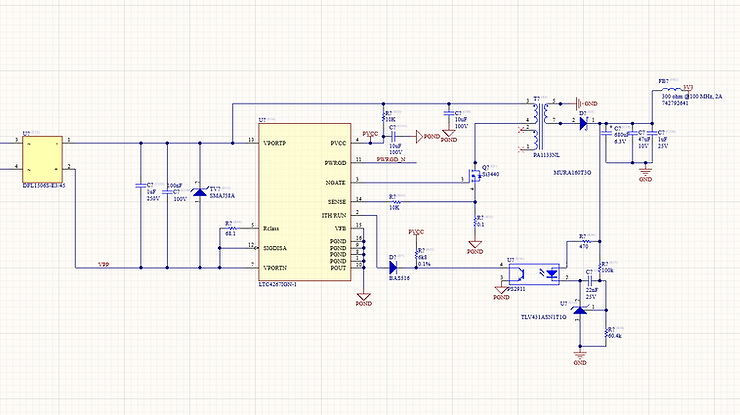
Typical PoE solution using the LTC4267 from Analog Device
Galvanic Isolation Is Not High-Frequency Isolation
An optocoupler provides galvanic isolation, meaning there is no direct conductive path between its input and output.
However, at high frequency, isolation is dominated not by conductivity, but by capacitance.
Inside every optocoupler there is:
-
Parasitic capacitance between the LED and the photodetector
-
Parasitic capacitance between package pins
-
Parasitic capacitance to surrounding copper and planes
Typical values are small — often in the range of 0.5 pF to several pF — but at high dv/dt these values become critically important.
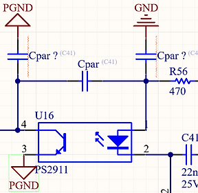
When we add an optocouple we should always imagine the 3 parassitic capacitors as shown above.
The Role of High dv/dt Nodes
In switching power supplies, nodes such as the drain of a MOSFET or the primary switch node ( Vsw) experience extremely fast voltage transitions.
dv/dt values of tens of volts per nanosecond are common.
Any parasitic capacitance connected to these nodes will inject displacement current according to:
I=C⋅dV/dt
Even a few picofarads can result in tens or hundreds of milliamps of current spikes at each switching edge.
These currents do not flow through wires — they flow through electric fields.
How PCB Layout Makes the Problem Worse
The PCB often contributes far more parasitic capacitance than the optocoupler itself.
Common contributors include:
-
Pads and copper areas near Vsw
-
Test pads
-
Unused footprints
-
Copper pours under or near switching nodes
-
Planes on adjacent layers
As shown in the figure below, even ten small pads can easily add 1–2 pF of parasitic capacitance.
Individually insignificant copper features become significant when they are all exposed to the same high-dv/dt node.
Figure 1 – Parasitic capacitance created by pads and copper near a high-dv/dt switching node
How the Noise Reaches the Optocoupler
The noise does not travel through the optocoupler in the schematic sense. It jumps across it capacitively.
The mechanism is as follows:
-
The high-dv/dt switching node couples capacitively to nearby copper
-
Displacement current is injected into the secondary-side ground or feedback network
-
The optocoupler input and output no longer share a stable reference
-
The optocoupler output current is modulated by noise
-
The feedback loop reacts to noise instead of true output voltage
This happens even though there is no DC connection across the isolation barrier.
Why the Feedback Loop Suffers So Much
The optocoupler output typically feeds:
-
An error amplifier
-
A compensation network
-
A high-impedance control input
These circuits are:
-
High gain
-
High impedance
-
Extremely sensitive to injected current
As a result, very small parasitic currents can cause:
-
Output voltage jitter
-
Loop instability
-
Subharmonic oscillation
-
Audible noise
-
EMC failures that appear random or load-dependent
Why This Is Hard to Diagnose
This problem is often misdiagnosed because:
-
The schematic shows perfect isolation
-
DC measurements look correct
-
The problem may only appear at high line or high load
-
EMC failures
-
Adding snubbers or capacitors sometimes “helps” by accident
-
audible noise
Without understanding the capacitive coupling mechanism, fixes are often trial-and-error.
Practical Layout Rules for Optocouplers
To minimise parasitic noise injection into optocouplers:
-
Keep high-dv/dt copper areas as small as possible
-
Avoid pads, vias, and copper pours near Vsw
-
Do not place planes under switching nodes or transformers
-
Keep optocoupler input and output circuitry compact and local
-
Treat optocouplers as high-frequency analog components, not digital isolators
-
Physically separate switching nodes from feedback and opto circuitry
These measures reduce parasitic capacitance and therefore reduce displacement current.
Key Takeaway
Optocouplers do not fail because they are bad components.They fail because parasitic capacitance turns isolation into a high-frequency coupling path.
In switching power supplies, controlling dv/dt and parasitic capacitance is just as important as choosing the right topology or controller.
The schematic shows isolation.
The PCB determines whether that isolation survives at high frequency.
Written by Francesco Poderico
More on Electronics
Electronics
Estimating the Lifetime of a Varistor on the Mains – What an Electronic consultant should know!
Introduction Varistors (typically MOVs) are widely used on mains lines for surge / transient protection. Under normal conditions they are passive, but when high‐voltage transients (switching surges, lightning induced, line overvoltage) occur, the varistor conducts, clamps the voltage and absorb
Francesco Poderico · · 2 min read
Electronics
Conductive Emissions due to lack of Bulk Capacitors
In one of my previous blogs, I discussed the importance of adding common mode filtering to power cables. Nevertheless, even the best filtering may not be enough to pass CE. When this occurs, most EMC testing houses recommend using "low frequency" ferrites, like Fair-Rite's excellent Material 31, whi
Francesco Poderico · · 3 min read
Electronics
Conductive emissions issues due to rectifier diodes
There is a feeling in me that sometimes the old books are better than the new ones. As an example, a book by Hnatek called Design of Solid State Power Supplies might be one of those gems that shouldn't be missed in your library if you are interested in solid-state power supplies. This old book s
Francesco Poderico · · 3 min read