
Some analysis I do when I design a DCDC converter. (Part 4)
Francesco Poderico · · 2 min read
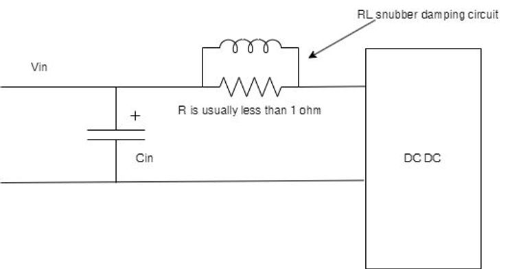
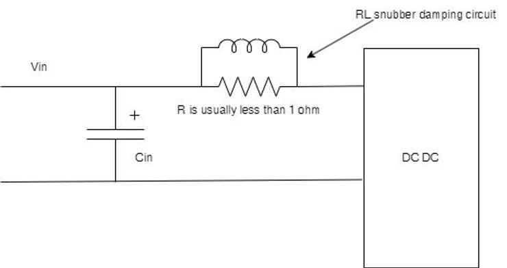
As we have seen in parts 1, 2, and 3, the input current loop of a DCDC converter affects both conductive and radiated emissions. Furthermore, the output current loop primarily affects radiated emissions.We then learned how an R/C snubber works and how antiparallel output capacitors can reduce radiated emissions.In the next section, we examined how the input voltage and an R/C on the boot pin of a DCDC converter affect the emission in the 30-300 MHz range. The second type of snubber I want to discuss today is the RL snubber damping.If you have read part 2, you should understand how the RC snubber works.Question: "Is it possible to achieve the same without affecting the output current loop area?"There is a relatively straightforward procedure for doing so, and the answer is yes.The snubber here is less obvious than the one we saw previously.As a rule, we prefer having an impedance between the Cin and the switching circuit that is as small as possible at lower frequencies, but we do not mind if it is one ohm (ish) at higher frequencies.This can be achieved by placing an inductance in parallel with your resistor R to achieve the desired result.If the inductance is low at a lower frequency, then the impedance is low, but as the frequency increases, the impedance will. There may be a time when you have seen this circuit in some design and wondered how it works or how it works.
Have seen in some design and if you wondered how it works. You now have the answer to your question. Initially, it may not seem intuitive, but once you get the hang of it, you will find it to be a very simple process.
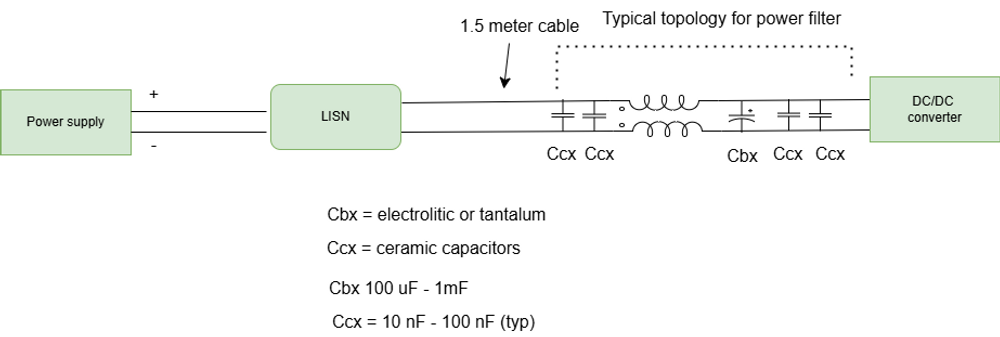
In order to design a DCDC converter, you will need the following information:1. Identify all the current loops and make them as small as possible2. Add enough filtering (on both ends) to ensure all the harmonics of interest are within those loops.3. Possibly evaluate using an input common mode choke or a Pi filter at the input.4. estimate the radiated emission (see part 1)5. play with duty cycle and rise time and fall time (RC on the boot pin)6. add an RC snubber damping7. add an LR snubber damping8. add do not fit ferrite at input and outputSo, as you can see, there are many decisions to make. In my working experience, I have noticed that most people do point 1 correct and then fail in most or all other points. If you have read my posts, you now have an arsenal of solutions you can use in your design.
Written by Francesco Poderico
More on Electronics
Electronics
How Parasitic Capacitance Breaks Optocoupler Isolation in Switching Power Supplies
Optocouplers are widely used in isolated power supplies to transfer feedback information across an isolation barrier. In schematics, they appear as a clean and robust solution: no galvanic connection, clear separation between primary and secondary, and good noise immunity. In practice, optocouplers
Francesco Poderico · · 3 min read
Electronics
Estimating the Lifetime of a Varistor on the Mains – What an Electronic consultant should know!
Introduction Varistors (typically MOVs) are widely used on mains lines for surge / transient protection. Under normal conditions they are passive, but when high‐voltage transients (switching surges, lightning induced, line overvoltage) occur, the varistor conducts, clamps the voltage and absorb
Francesco Poderico · · 2 min read
Electronics
Conductive Emissions due to lack of Bulk Capacitors
In one of my previous blogs, I discussed the importance of adding common mode filtering to power cables. Nevertheless, even the best filtering may not be enough to pass CE. When this occurs, most EMC testing houses recommend using "low frequency" ferrites, like Fair-Rite's excellent Material 31, whi
Francesco Poderico · · 3 min read