
Some analysis I do when I design a DCDC converter. (Part 2)
Francesco Poderico · · 3 min read
I had the pleasure of working with a customer a few years ago, who was ready to launch his product on the market. My suggestion was to go for full CE compliance before the test and to contact me only if there were any problems that occurred during the test.
As the EMC house was just 15 minutes away from my old office, I made sure to let him know that I was available all day if they had any issues, and I would only answer if something was wrong. At about 9:30 am, I received a call from Francesco... "Francesco, would you be able to come to the EMC lab, please? We are over our limit at the moment."
Once I arrived at the location, I asked for a schematic and a PCB layout, and from the radiation emission, I was able to establish that it was most likely the DCDC converter that was the cause of the problem (I have discussed in the past the typical emission shape of a DCDC converter). During the design process, there were three mistakes that were made.
1. The snubber is not present (sometimes referred to as the boot circuit)
2. There is no ground plane (this is one of the classics)
3. Having a lack of understanding of what the two main current loops in a DCDC converter are
In today's article, I will only be discussing points 1 and 3 of the list.
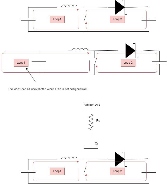
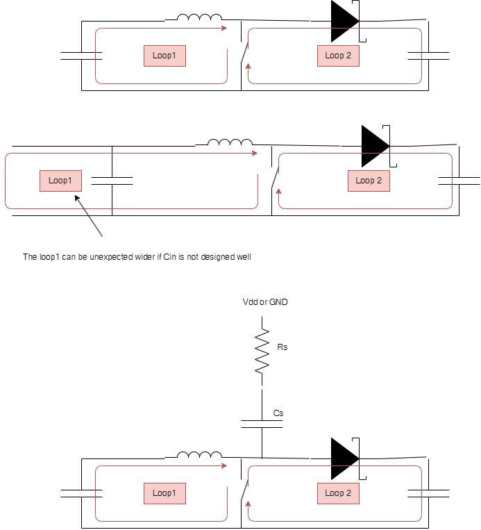
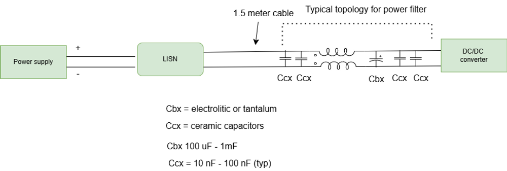
First of all, let's take a look at point 3. In order to design a DCDC converter, you have to create two main current loops, one at the output and one at the input. My drawing shows an input loop and an output loop that can be easily identified if you look at it closely. As discussed in the first part of this series, the loops should be as small as possible. However, when you miscalculate either the input or output capacitors, you are able to "elongate" the loop, and as a result, you will either have radiated emission or conductive emission levels that are above what is safe. As you can see in the drawing I made, there is a possibility of a problem occurring when the input capacitor is too low. When this happens, the loop may suddenly go back up to the power supply, and the chances are that if we are trying to perform conductive emission on those wires, we may fail. This is something that I have seen on a number of occasions. You need to be very careful here; you need to contain the loop as much as possible within the frame of your Cin and your DCDC converter. As a rule of thumb, the Cin usually requires a large capacitor (not LESR) and several good quality LESR ceramic capacitors.
I don't use the bulk capacitor with LESR in order to avoid overvoltage, which can happen when you plug in a power supply without outrushing current control to the equipment you are powering.
In other words, a mistake on the Cin may result in issues with conductive emissions... on the other hand, what if you have followed everything in the manual and you still don't pass the radiated emissions test? Let us assume that we still fail even though I made some suggestions in Part 1.
The best solution for this issue would be to use a snubber and lose some of the efficiency of the DCDC converter in this situation. Snubbers are RC circuits that are usually applied near the driving NMOS (see my illustration for a brief description). You are trying to reduce the high harmonics from the switching regulator by slowing down the rising and falling edge of the switching regulator.
One of my customers once called me and told me he had a design engineer calling from one of his customers... he used to refer to this kind of design as "Francesco's stuff" and once he called me ... So Francesco, what is that "Francesco's stuff" near the DCDC converter all about? It was actually this snubber that did it... :-)
I think once you know what it does it is very easy to understand.
Written by Francesco Poderico
More on Electronics
Electronics
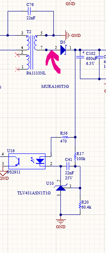
How Parasitic Capacitance Breaks Optocoupler Isolation in Switching Power Supplies
Optocouplers are widely used in isolated power supplies to transfer feedback information across an isolation barrier. In schematics, they appear as a clean and robust solution: no galvanic connection, clear separation between primary and secondary, and good noise immunity. In practice, optocouplers
Francesco Poderico · · 3 min read
Electronics
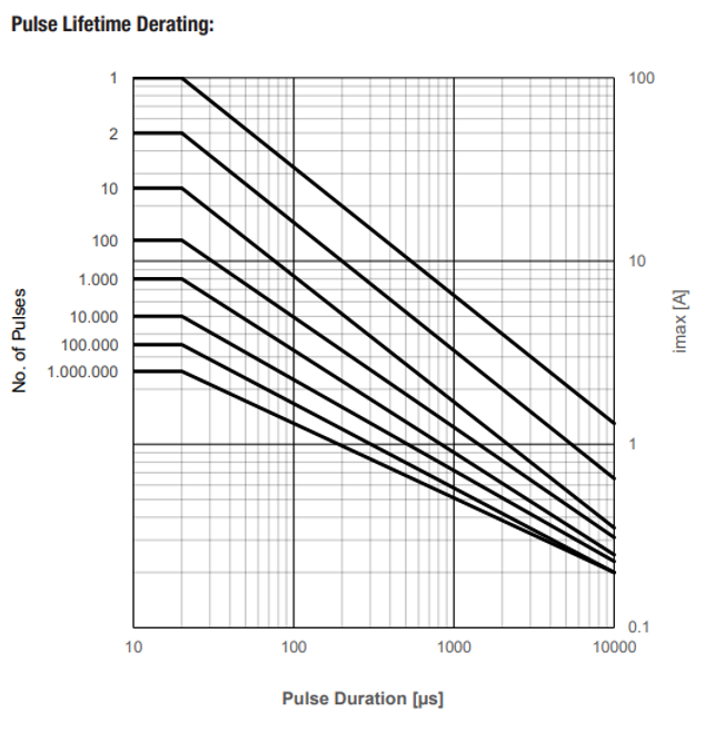
Estimating the Lifetime of a Varistor on the Mains – What an Electronic consultant should know!
Introduction Varistors (typically MOVs) are widely used on mains lines for surge / transient protection. Under normal conditions they are passive, but when high‐voltage transients (switching surges, lightning induced, line overvoltage) occur, the varistor conducts, clamps the voltage and absorb
Francesco Poderico · · 2 min read
Electronics
Conductive Emissions due to lack of Bulk Capacitors
In one of my previous blogs, I discussed the importance of adding common mode filtering to power cables. Nevertheless, even the best filtering may not be enough to pass CE. When this occurs, most EMC testing houses recommend using "low frequency" ferrites, like Fair-Rite's excellent Material 31, whi
Francesco Poderico · · 3 min read