
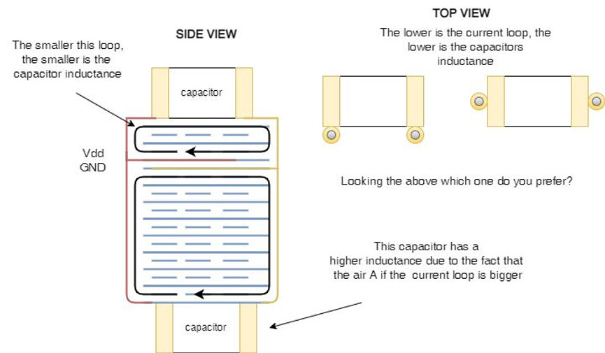
When we place our bypass capacitors on a PCB, there are several factors that may affect the series inductance of the capacitor ESL when it is placed on the board. What can we do in order to minimize it during the routing of our PCB? Do you consider the footprint of the capacitor when you select the capacitor?Yes, there are a few things that can be done in order to solve this problem. The first thing we need to do is look at the footprint. A general rule of thumb is that the smaller the footprint, the smaller the equivalent series inductance (ESL). A look at the capacitor datasheets will enable you to verify this easily. It must be noted, however, that I have not seen many application notes that describe the optimal way to route the bypass capacitor. In addition, I have not come notfoundn any application notes that explain why routing A is better than routing B.As I usually do, I will explain what I mean with an example to help you understand. I have made a drawing that I would like you to see. Accordingly, the smaller the loop we create and the smaller the ESL, the more you would agree with what we studied at school or university. It is clear from these numbers that the capacitor at the top layer has a lower ESL than lower the capacitor at the bottom layer, because the distance between the capacitor and the VDD/GND layers is smaller than the distance between the capacitor at and the VDD/GND layers. Moreover, you will see that routing the vias on the pad side is better than routing them on the edge (we make the loop smaller by routing them on the pad side).Therefore, it can be said that ESL is largely determined by the following factors:There is also the physical dimension of the via (which is not discussed in this article)In relation to the pads, the position of the via is critical.GND/Vdd plane distance (the longer the distance, the worse it is)I hope you enjoyed it! Bye now!
Post Button
Chat
Contact Us
loadbalancer.visitor-analytics.io
loadbalancer.visitor-analytics.io is blocked
Written by Francesco Poderico
More on PCB
PCB
EMC Troubleshooting Part 3 — Broadband Footprints: 2‑Layer Boards & Plane Slots
Scope: Why some products show broadband radiated emissions from 30 MHz–1 GHz, why issues often persist up to 400 MHz–1 GHz even on multilayer boards, and how to prove and fix the root cause fast. 1) What “broadband” really means in RE On the plot, broadband looks like a wide hum
Francesco Poderico · · 4 min read
PCB
High-Speed Vias: Why Solid Ties Beat Thermal Reliefs
Thermal-relief “spokes” help solderability, but they add inductance and cut slots in your reference plane—exactly where high-frequency return current needs a short, wide path. For HDMI, PCIe, and other multi-GHz links, prefer solid connections to ground on anything that carr
Francesco Poderico · · 2 min read

PCB
Conductive Immunity failure due to a two layers stack PCB
Over the last ten years, I have seen so many PCBs fail conductive immunity that I could write a book about it. In most cases, the errors are caused by bad designs and a lack of understanding of the ground plane's role. Since I keep seeing people recommend designing 2 layers PCBs to save a few pence,
Francesco Poderico · · 2 min read