
I designed my first general I/O PCI card when I was a student (a few years ago now :-)). The PCI card was part of my thesis, and the design was challenging at the time. One of my professors was quite impressed with my throughput. The FIFO was bigger than I needed, and I managed to get all the data out without the card getting too warm! Despite some errors, the card worked.
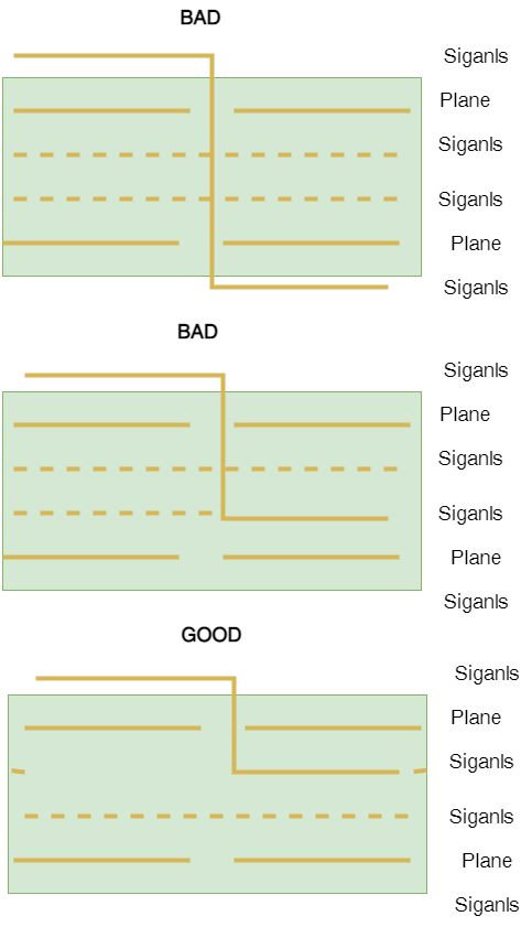
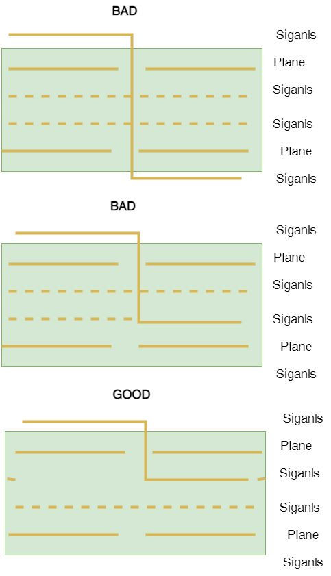
What is the reason for my saying that? As a result of the design, I made some mistakes that I wasn't aware of at the time, and I would like to discuss them with you today.The error occurs every now and then and I see it every now and then. It usually happens when the PCB layout engineer does not receive all the information that was provided by the electronic designer, or when the return current on a high-speed trace is not fully understood by the engineer responsible for its layout. Since I work as a consultant, I do not have to deal with this kind of issue; this is a nice aspect of being a consultant, as I am able to design everything by myself, but this is not always the case, sometimes designs are so complex that you have to hire a team of engineers. It is important that if this is your situation you explain to the PCB layout engineer the criticality of each signal from the perspective of SI as well as EMI if this is the caseRegardless, to get back to the topic, keep an eye on the return current path when you change layers! There are a few posts in which I have mentioned this; however, based on some comments, I had the impression that someone was unfamiliar with the subject matter. It has been discussed previously how stitching vias are stitched between the GND planes, as well as between different power planes and power zones. However, it is possible in some cases that we may not be able to add stitching vias in certain areas of our PCBs. In that case, what should we do? Take a look at the drawing below. As you can see in the first drawing (top), I drew a critical line from the top layer to the bottom layer of the first drawing. Because I did not add any stitching vias between the 2 GND planes, the return current is uncontrolled, and this may lead to a common mode current and SI issues, since there are no stitching vias between the 2 GND planes.It should be noted that in the second drawing, I still make the same type of mistake, although it is somewhat less pronounced than in the first one.As you can see in the final drawing (bottom), I have the correct routing" because the return current is shared on the same plane, this is what you should aim for in your design. If at all possible, keep the return current on the same plane.As such, if stitching vias can't be added, you should use the same reference plane (GND or Vdd, it doesn't matter). This is the best possible strategy from a SI and EMI point of view.I hope you have found this interesting! Bye now!
Written by Francesco Poderico
More on PCB
PCB
EMC Troubleshooting Part 3 — Broadband Footprints: 2‑Layer Boards & Plane Slots
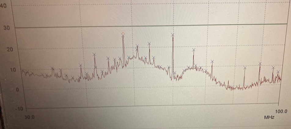
Scope: Why some products show broadband radiated emissions from 30 MHz–1 GHz, why issues often persist up to 400 MHz–1 GHz even on multilayer boards, and how to prove and fix the root cause fast. 1) What “broadband” really means in RE On the plot, broadband looks like a wide hum
Francesco Poderico · · 4 min read
PCB
High-Speed Vias: Why Solid Ties Beat Thermal Reliefs
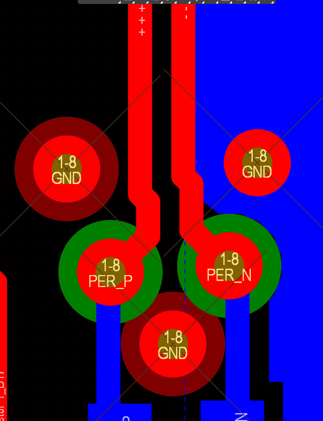
Thermal-relief “spokes” help solderability, but they add inductance and cut slots in your reference plane—exactly where high-frequency return current needs a short, wide path. For HDMI, PCIe, and other multi-GHz links, prefer solid connections to ground on anything that carr
Francesco Poderico · · 2 min read

PCB
Conductive Immunity failure due to a two layers stack PCB
Over the last ten years, I have seen so many PCBs fail conductive immunity that I could write a book about it. In most cases, the errors are caused by bad designs and a lack of understanding of the ground plane's role. Since I keep seeing people recommend designing 2 layers PCBs to save a few pence,
Francesco Poderico · · 2 min read