
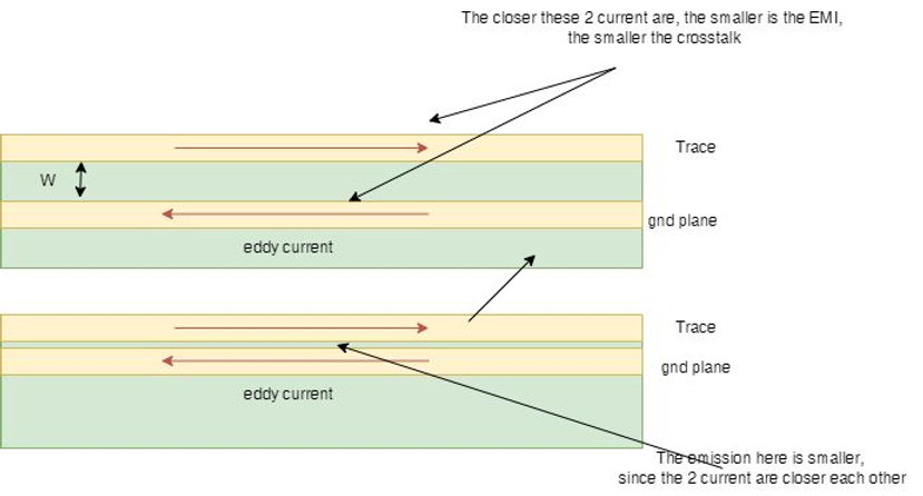
To avoid EMI and crosstalk on both PCB traces and connectors, it is crucial to understand the return path current.
Previously, I discussed how a ground plane reduces EMC problems (both emission and immunity). In addition to minimising crosstalk, a ground plane helps minimise interference. You know I believe you don't know a subject well if you can't explain it using a simple example. Therefore I'll explain this using just words and not formulas. If you want to dig into the matter, let me know in the comments, and I'll suggest a few books.
I made this drawing for you to see. Eddy currents are generated when a current is carried on a trace by the ground plane underneath it. This is well known, and I have discussed this already.
Magnetic fields will be created in opposite directions by these two currents.
You can see that in the second drawing (bottom), the two currents are closer together and, as a result, we should expect a weaker magnetic field than in the first example.
Consider a case where w=0 and both currents overlap, in which case there is no magnetic field created.
As a result, the smaller the ground plane, the lower the magnetic emission, and therefore, the lower the crosstalk.
This kind of design detail is essential these days when we have microcontrollers, sensors, FPGA, DDR, etc., on the same board. Minimising the crosstalk between traces is vital today, and understanding your tools is very important.
So... to recap... a ground plane not only improves the radiated emission, radiated immunity, conductive emission and conductive immunity but also has a crucial role in reducing the crosstalk between traces.
I hope you enjoyed it.
Written by Francesco Poderico
More on PCB
PCB
EMC Troubleshooting Part 3 — Broadband Footprints: 2‑Layer Boards & Plane Slots
Scope: Why some products show broadband radiated emissions from 30 MHz–1 GHz, why issues often persist up to 400 MHz–1 GHz even on multilayer boards, and how to prove and fix the root cause fast. 1) What “broadband” really means in RE On the plot, broadband looks like a wide hum
Francesco Poderico · · 4 min read
PCB
High-Speed Vias: Why Solid Ties Beat Thermal Reliefs
Thermal-relief “spokes” help solderability, but they add inductance and cut slots in your reference plane—exactly where high-frequency return current needs a short, wide path. For HDMI, PCIe, and other multi-GHz links, prefer solid connections to ground on anything that carr
Francesco Poderico · · 2 min read

PCB
Conductive Immunity failure due to a two layers stack PCB
Over the last ten years, I have seen so many PCBs fail conductive immunity that I could write a book about it. In most cases, the errors are caused by bad designs and a lack of understanding of the ground plane's role. Since I keep seeing people recommend designing 2 layers PCBs to save a few pence,
Francesco Poderico · · 2 min read