

Over the last ten years, I have seen so many PCBs fail conductive immunity that I could write a book about it. In most cases, the errors are caused by bad designs and a lack of understanding of the ground plane's role.
Since I keep seeing people recommend designing 2 layers PCBs to save a few pence, I decided to write an article to explain why this is usually a bad idea.
I'm not saying you should never do it; I'm just giving you the tools to make your own decisions. After that, you can decide whether you want to take the risk of saving a few pennies or not.
You may ask me.
Francesco, I understand that we may have emission issues by not using GND/VDD planes, but why do we have immunity issues?
This is an excellent question. Let's see how a conductive immunity test is usually done.
During the conductive immunity test on some cables of your EUT (Equipment Under Test), the testing house needs to inject some common mode signal on many cables. For example, to the power cable, to the data cables, if you have some sensors, even those cables are tested, and so on!
This signal has a frequency range that usually goes from 150 kHz up to 30MHz ( it can be different, sometimes, the lower end is 9 kHz, and the upper end is 80 MHz). Most of the time, a 1 kHz sinewave is AM modulated on it.
Now, let's say you have been very careful on every aspect of the design, except one; you decided to use a 2 layers PCB.
Let's see what may happen from an immunity stand of view.
Let's consider FIG.1
Since we have a two-layer PCB, every chip "GND" is probably connected using a track and maybe a few vias.
A trace between each PCB trace means that we have an inductor much higher than we would have achieved with a nice plane between each GND pin.

FIG.1 On a PCB without a solid GND reference.
During conductive immunity testing, let's see what might happen.
As I have just mentioned, we inject some noise into all our harnesses during the test.
What do you think will happen to the GND all over the PCB?
As the track gets longer, the GND "noise" will get bigger and bigger until, eventually, the chip will misbehave.
I fix 40% of designs that are two layers of PCBs because the designer did not understand the physics behind this decision.
My advice is to be very careful, if you go for a 2 layers PCB you may get hit by any sort of issue. The issue that I have discussed today it's just the simplest one to explain.
Not sure yet?
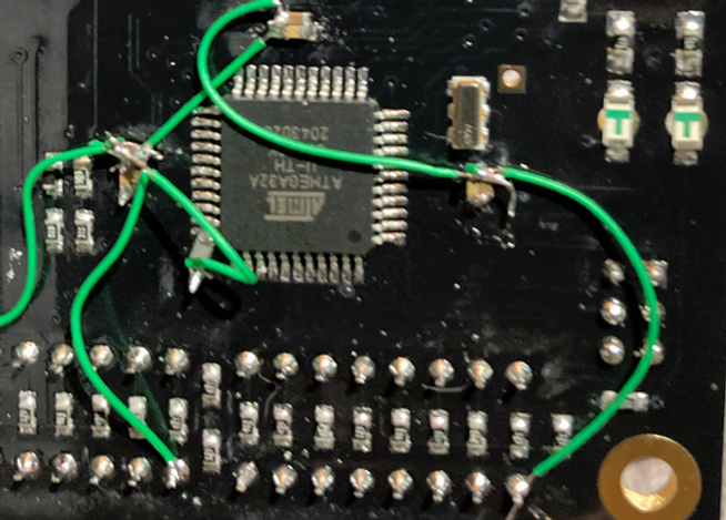
This is what I had to do once to show a customer how minimizing the inductance you see above improves the conductive immunity of its product.
Written by Francesco Poderico
About the author
These articles are Francesco Poderico's work. He built EMC Design Solutions around a simple idea: EMC is not black magic, and every failure has an explanation. When he closed the company, he passed his writing to us so it could keep helping engineers. We publish it unchanged.
Facing a problem like this one?
We help hardware teams find the root cause and pass. Start with a call, or map the rules that apply to your product first.
More on PCB
PCB
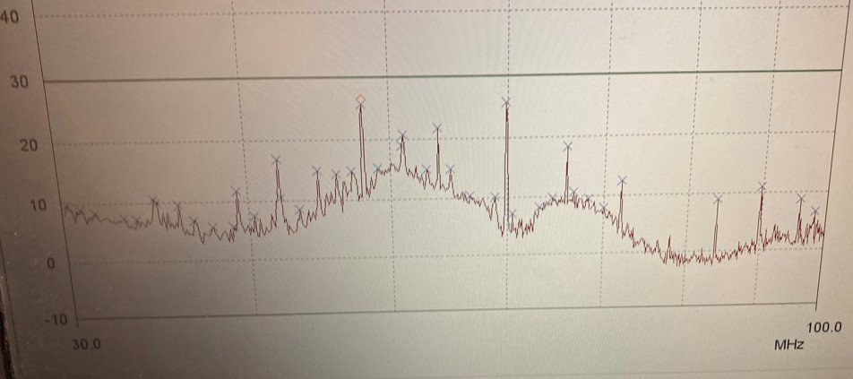
EMC Troubleshooting Part 3 — Broadband Footprints: 2‑Layer Boards & Plane Slots
Broadband humps from 30 MHz to 1 GHz usually mean large current loops or apertures. Why 2-layer boards and slotted planes cause them, how to prove it at the lab, and how to fix it.
Francesco Poderico · · 4 min read
PCB
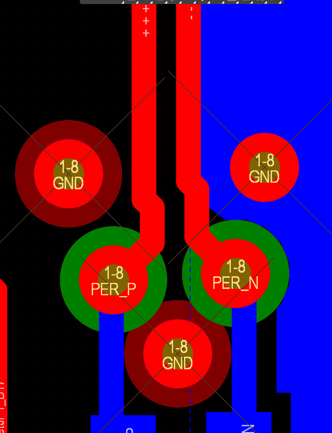
High-Speed Vias: Why Solid Ties Beat Thermal Reliefs
Thermal-relief spokes help soldering but add inductance and cut slots in the reference plane. Why to use solid ground connections on RF returns for HDMI, PCIe and other fast links.
Francesco Poderico · · 2 min read
PCB
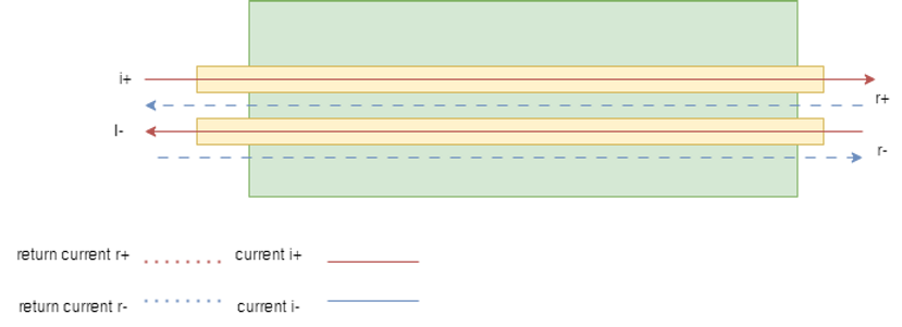
Radiated emissions due to split planes.
Differential signals like USB or RS-485 do not forgive routing over a split plane. Why crossing a gap creates radiated emissions and how to route it correctly.
Francesco Poderico · · 3 min read